Feminist hacklab Mz* Baltazar’s Lab built ATmega328P-compatible PCBs from wild-dug clay, open-fire kiln, and urban-mined silver paint.
Key Takeaways
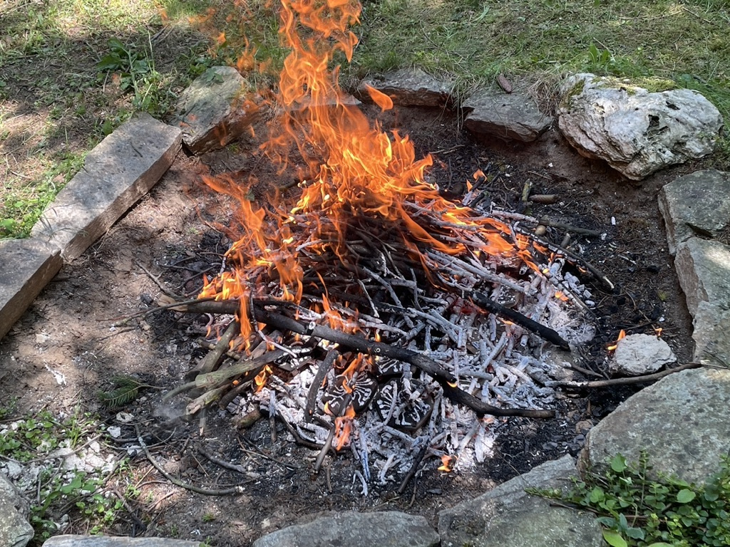
Base substrate is locally sourced natural clay, shaped with a hexagon tile cutter, dried for 24 hours to two weeks, then fired at ~700°C in a backyard wood fire.
Circuit traces are hand-painted with silver paint made from waste silver powder collected by jewellers, chosen because it survives 700°C and stays conductive despite oxidation.
ATmega328P chips salvaged from broken Arduino Uno boards are reused; the project explicitly targets conflict-mineral reduction in electronics.
A 3D-printed stamp imprints the circuit layout directly into wet clay before drying, eliminating the need for chemical etching or photoresist.
Hexagonal tile format was intended to allow boards to tile together electronically, but was abandoned because straight edges proved too inconsistent with this material.
Hacker News Comment Review
The core technical debate is whether the clay substrate adds any sustainability benefit at all: multiple commenters argue point-to-point or wire-wrap soldering eliminates the need for any substrate, making the clay PCB a greenwashing layer on top of an unnecessary step.
Commenters explored lower-energy alternatives that skip the kiln entirely: wood plank substrates with copper tape, pine rosin adhesive for copper laminate, and air-drying clay with a finer-grained 3D-printed or CNC stamp.
The project connects to a documented lineage of lo-fi PCB alternatives, including MIT Media Lab’s High-Low Tech group and kit-of-no-parts work from Hannah Perner-Wilson and Leah Buechley circa 2010.
Notable Comments
@jna_sh: Participated in the workshop at Creative Coding Utrecht; clay sourced partly from Vienna metro excavations – confirms the local-mining ethos is practiced, not just claimed.
@atoav: Electronics lab perspective: “Better than a greenwashed alternative is to avoid using material that is not necessary” – flags that durability calculus (one lasting board vs. ten disposable ones) matters more than substrate choice.
@itsdesmond: Directly links to MIT Media Lab High-Low Tech group and copper-electroplated clay dead-bug circuits as prior art.