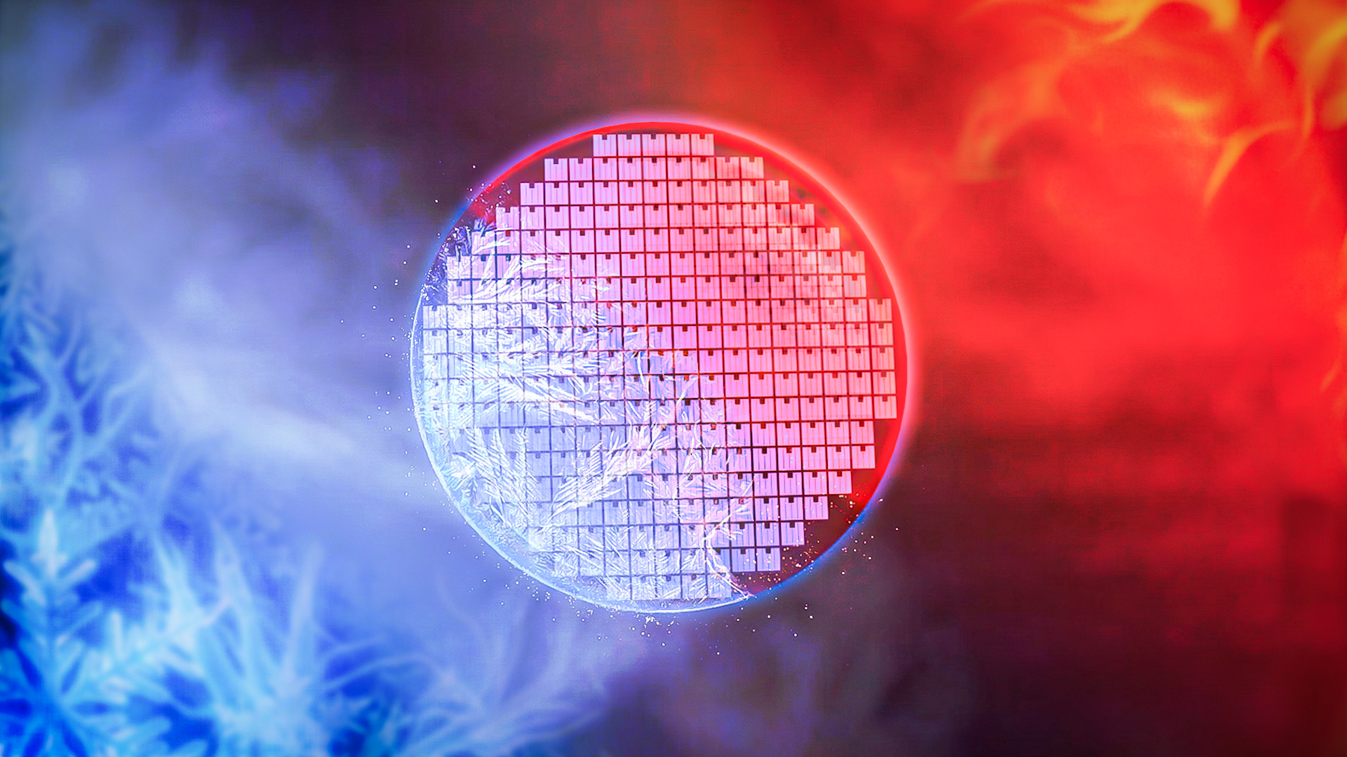
KAUST paper demonstrates beta-gallium oxide FinFETs and logic inverters operating reliably at 2 K, the first ultrawide-bandgap semiconductor to do so.
Key Takeaways
Beta-gallium oxide (β-Ga2O3) avoids freeze-out at cryogenic temperatures via an impurity band created by silicon dopants, allowing current flow near absolute zero.
Two devices were validated at 2 K: a FinFET transistor and a NOT-gate inverter, both fundamental logic building blocks.
The same material works up to 500 °C and resists radiation, making it a single-material solution across extreme temperature ranges relevant to space probes.
Practical payoff: cryogenic quantum computing electronics and space hardware could shed bulky thermal management systems by using one semiconductor across the full operating range.
Next steps include RF transistors, photodetectors, memory cells, and scaling toward complex cryogenic chips; current demos are micrometer-scale.
Hacker News Comment Review
Discussion is thin; comments are mostly quips rather than technical critique, with no substantive debate on the physics, fabrication tradeoffs, or quantum-computing integration path.
One commenter flagged the micrometer scale of current devices and raised an open question about miniaturization limits, which the paper does not address.
Notable Comments
@biggerben: Links the original Nano Letters PDF and asks what the shrinkage limits are for micrometer-scale devices.