A 10-chapter build log covering a custom BCD scientific calculator on a Cyclone II EP2C5 FPGA, from CPU ISA design through a finished 3D-printed enclosure.
Key Takeaways
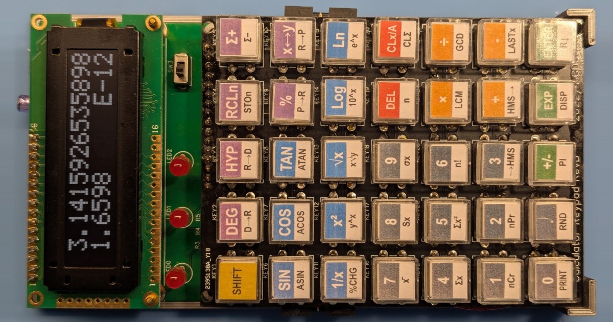
Uses binary-coded decimal internally, mirroring HP scientific calculator architecture; custom 12-bit fixed-length ISA with nibble-addressable memory and 14 ALU operations including 8086-style BCD-adjust.
Single Verilog source runs across ModelSim, Verilator, Qt desktop simulator, and WebAssembly without RTL changes, enabling test-before-hardware workflow.
2025 rewrite added guard digit, sticky bit, banker’s rounding, full trig suite, 10 STO/RCL registers, and hardware LFSR RNG validated against thousands of C++ reference vectors.
Final design fits in 1,593 logic cells, 35% of the EP2C5; custom PCB replaces dev board with JTAG and Active Serial programming connectors for fast iteration.
Honest postmortem: keypad feel falls short of vintage HP, TQFP-144 soldering was high-risk, and bench-to-portable gap was larger than expected.